Hacking The 3ds IV: Hardware attacks
Introduction
Let’s talk about hardware hacking, mostly targeting the Nintendo 3ds hardware, but certainly related to other distinct targets.
I have tried to create a post which explains with the maximum level of detail each attack / reversing procedure. I consider this useful as a learning resource for future generations. Moreover, it should also work as preservation for a lot of 3ds “scene” content back from as soon as 2011, which is getting lost and disappearing from internet; this includes images, posts, texts, plus some of my comments.
Hardware Attacks
A few years ago when I posted the first article about 3ds hacking I considered hardware hacking to be an obscure and complex learning field. Luckily, I’m very satisfied with what I have learned so far, and it no longer looks so frustrating. This has been possible because I have spent a certain amount of spare time investigating and learning, and also unexpectedly thanks to university, where I’m getting a lot of information about computer architecture. I want to share all this information.
The architecture of any console, like the 3ds, is composed by different electronics or hardware components. Depending on the information flowing through these components, we could consider them interesting for hacking. If we can attack a component and extract its information or make it behave as we wish, we say we have a working hardware attack. Of course there are tons of variations, so, to begin with, I will explain in general the concept of each attack and then apply the abstract idea to our target, the Nintendo 3DS.
Nand Dumping
For scene preservation purposes, I will start talking about Nand dumps. These have been a recurrent topic in the 3ds scene over the years.
What is a NAND memory?
A NAND memory is just a kind of flash memory chip based on NAND logic gates. As we saw in the first post, the 3ds uses an internal 1GB Samsung Nand Chip.
For example, some SD Cards are NAND memories, just that these are removable, while the 3ds one is soldered in the SoC. To learn how SD Cards work, read this nice document To sum up, sd cards can use a high speed mode, or a low speed SPI-based mode.
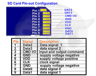
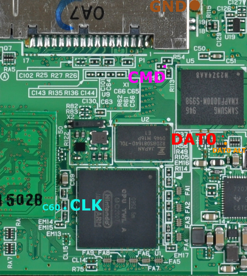
Explaining every detail about how flash memories are designed internally is out of the scope of this post. So as for now, let’s just consider how they work (in fast mode). Often we only need the following pins to do something like writing or reading their contents:
- CMD I/O
- One data line, for example DAT0 (to read the content in the memory address passed through the CMD I/O)
- CLK which is the clock signal
- VDD and GND to supply electricity to the chip.
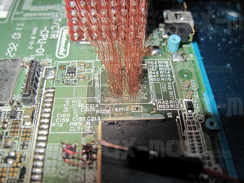
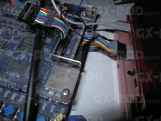
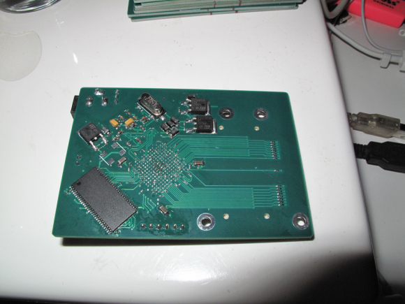
In the 3ds, these pins of the NAND chip were accessible from the board and so, we could solder to some pads or components in the board which were indirectly or directly connected to the NAND memory. This means there is no need to de-solder the memory just to read it (and usually the chips are difficult to de-solder and may break if you try to do it!).
This is the pinout for the Old3DS:
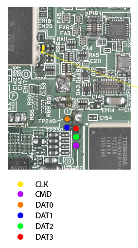
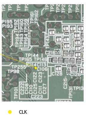
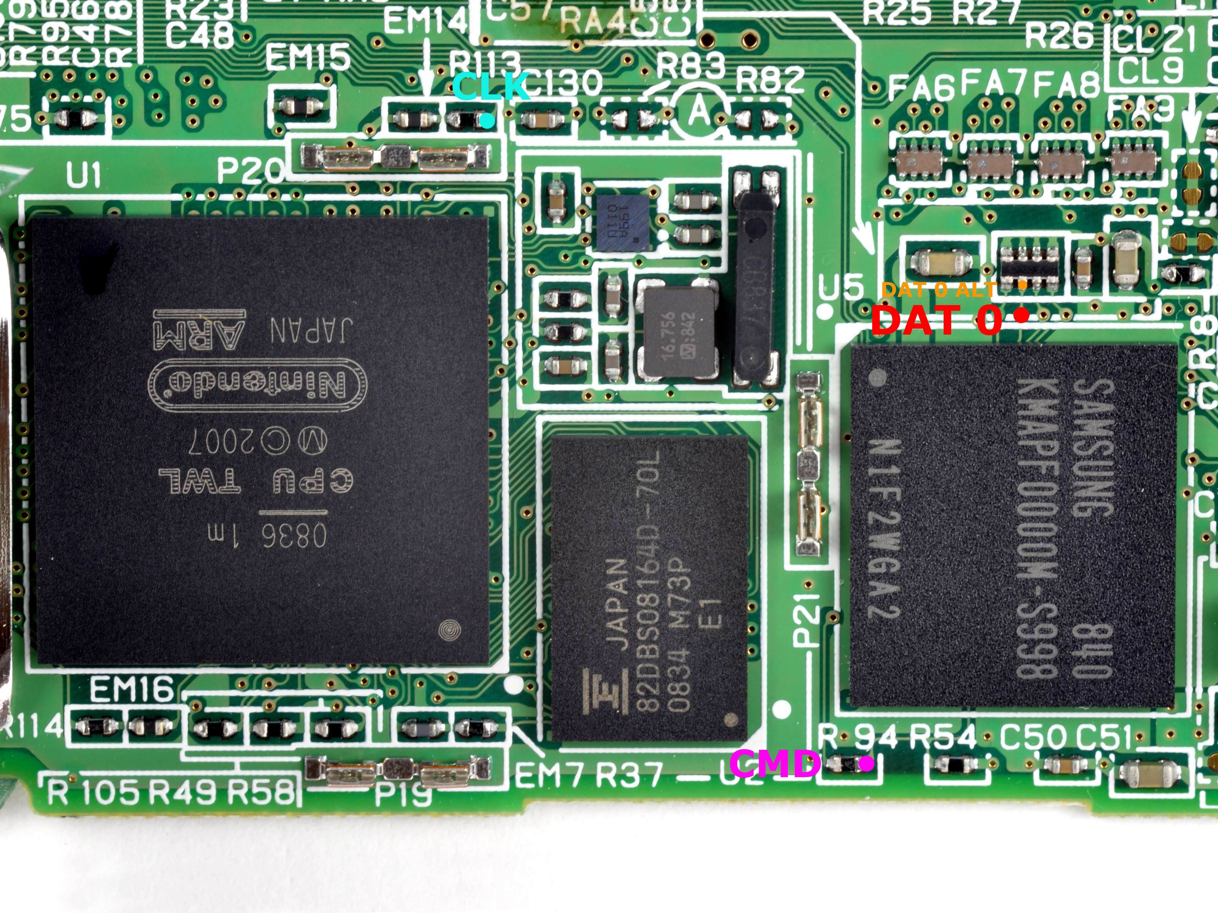
Main pins required, and an alternative pin for CLK in another part of the board.
Notice there is no VDD pin. This is because it is unnecessary. The chip doesn’t need to be powered externally, it will be powered properly if the console is turned on. As a bonus example, here is the pinout for the Nintendo DSi:
 Main pins required, and an alternative pin for DAT0 in another part of the board. (Top Dsi, Bottom DsiXL)
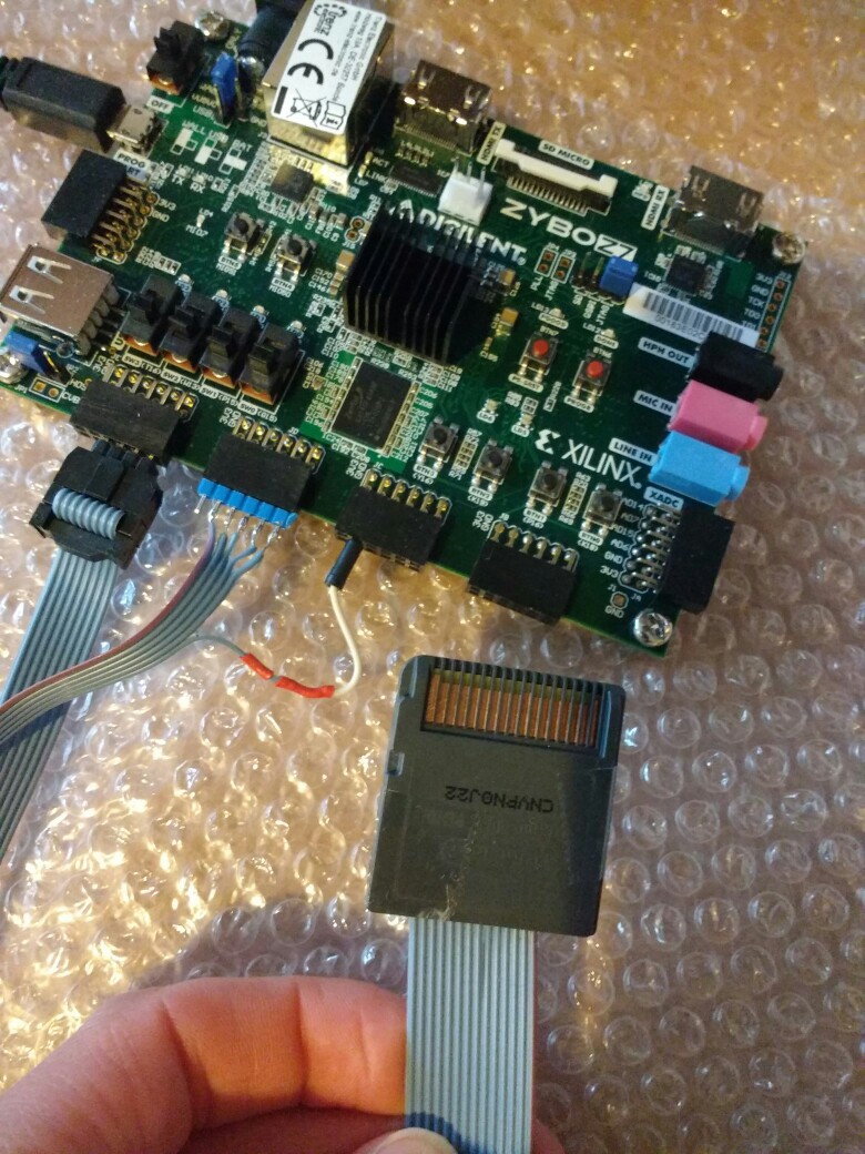
The last issue is getting to dump the contents to a computer. We could use some device like an Arduino, Raspberry Pi, or FPGA to implement the commands to talk with the SD or Nand memory, but there’s a better hack. How we do this? That’s actually the most straightforward part of all; we are crafting an adapter with cheap components and letting the computer’s OS handle the comunication.
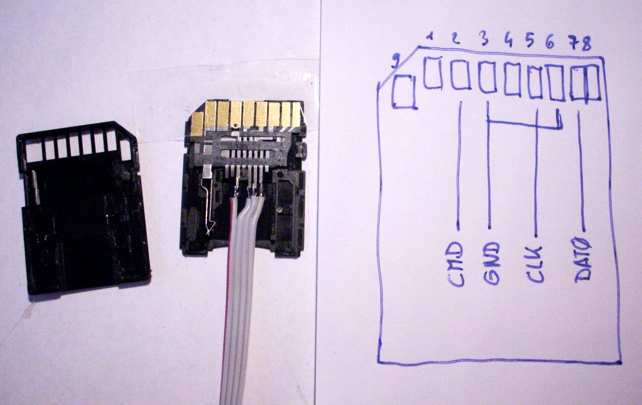
The concept is simple: We have seen that both an SD card and the NAND memory of the 3DS use the same protocol, right?. When you plug an SD card into the card reader of a computer, it sends the appropriate commands to initialize and read/write the card’s contents.
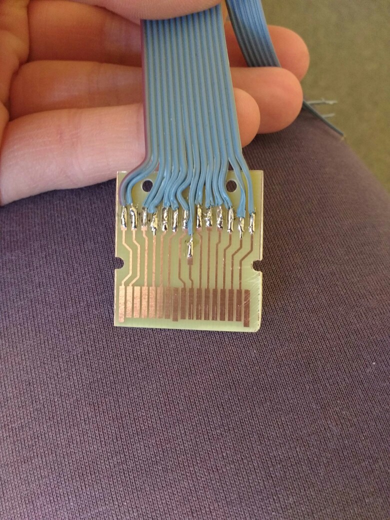
A more trivial example to make it clear. MicroSD cards also use the same protocol. An adapter from microSD to SD just connects the pins of the microSD to bigger pads so the SD reader of your PC can detect them. Now the question is, would a NAND to SD adapter actually work?. By connecting its pins to ones of the size of an SD card, can we just plug it to an SD reader in any computer? The answer is YES!. As you can see in the picture above this can be done modifying a dirt cheap microSD to SD adapter, soldering wires to its pins on one side, and soldering the other end of the wire to the pins in the 3DS board. And that’s it! The PC will talk to the NAND as if it were talking to an SD card. It appears as if it were a raw drive, we can just dump it with dd (on linux) or win32diskImager (on windows).
RAM Sniffing / RAM tracing and RAM injection
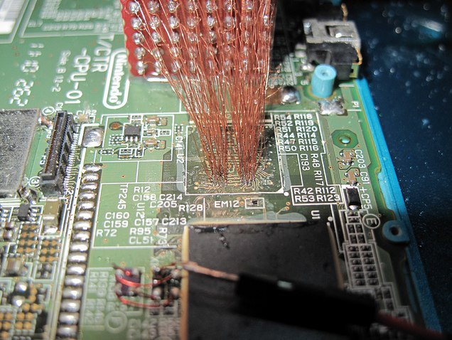
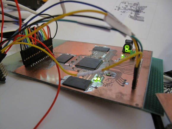
While the NAND read-write was simple, now I’ll feature a more complex attack. The concept is as follows; intercept the bus lines connecting the RAM chip to the board and trace writes and reads generating an “image” of the memory. This can be done with an FPGA.
This is known as RAM Tracing. The only console-hacking known attack of this kind was performed by @scamlime some years ago; she did it with the DSi’s RAM; find more information here, here, and here
Alternatively, the attack can be extended further, to the point that it allows injection or “emulation” of data blocks of the RAM. Not only requires the same hardware, an FPGA but also involves extreme soldering skills. We can create a setup to sniff the traffic as in attack 1, by hooking up to the chip lines. Specially, @scanlime hooked to the DSi’s CS (Chip Select) line of the board, and when it detected that the console was trying to read some data from the RAM, redirected it to her FPGA, providing the console with modified RAM data blocks. @scanlime’s work is by far the most open and documented setup, check it on the links above.
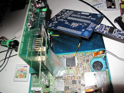
Injection of strings into RAM
Nevertheless I consider interesting to mention the work of neimod, who presumably was the first person ever to hack the 3ds. Here are some pictures of his work (now disappeared from the web) he used a custom fpga to do a similar attack but on the 3ds:


Update 2020: Some new recovered images
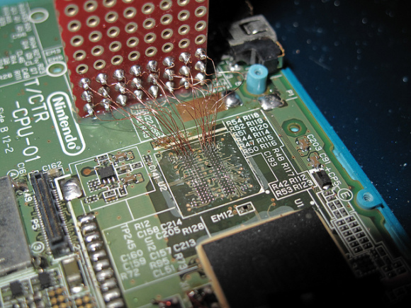
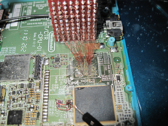
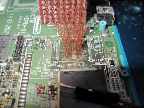
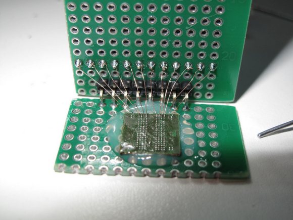
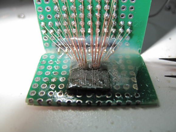
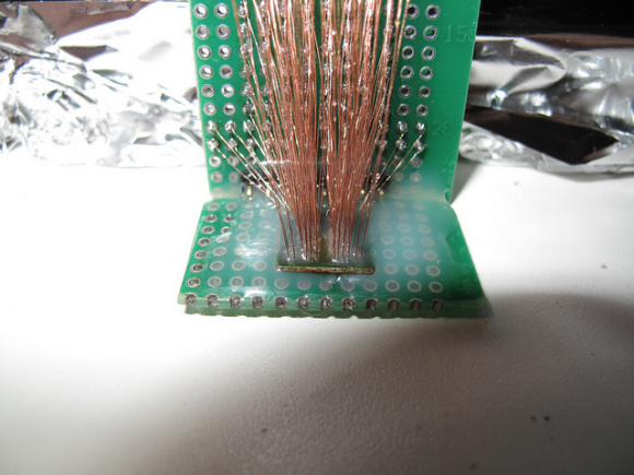
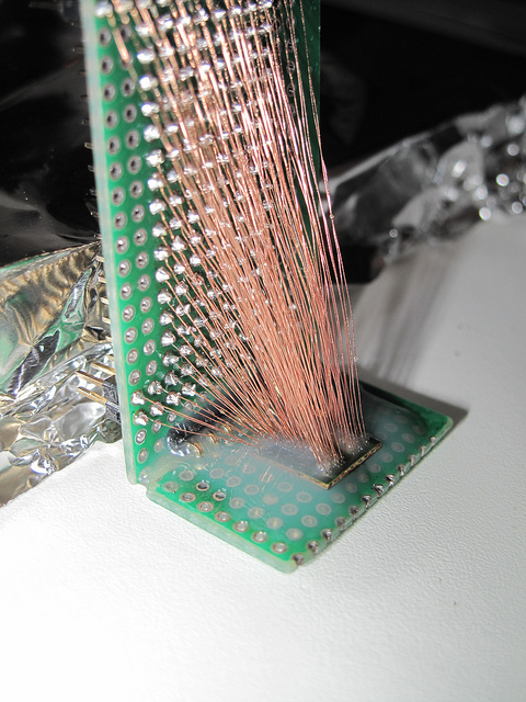
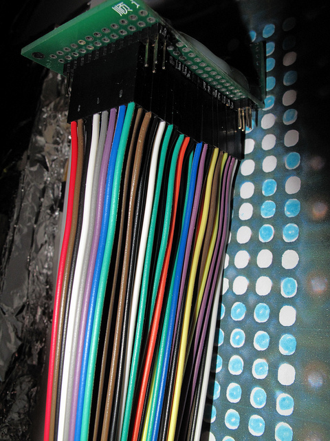

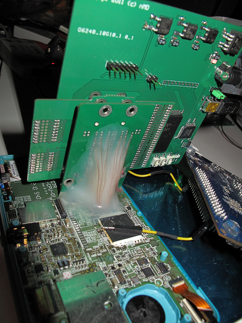
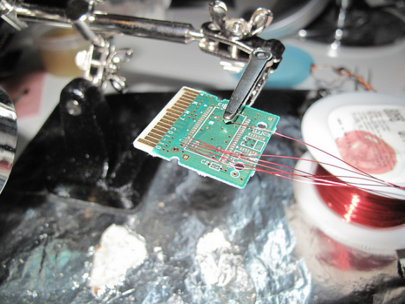

Unfortunately it is believed that neimod sold all his work. Later all the pictures were deleted but you can still see here some of the soldering work and setup used.
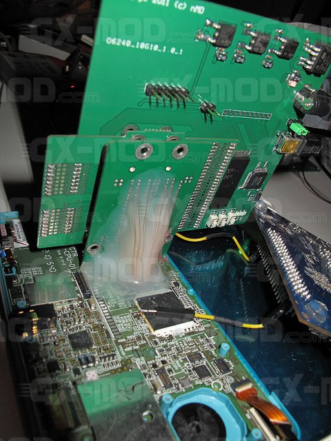
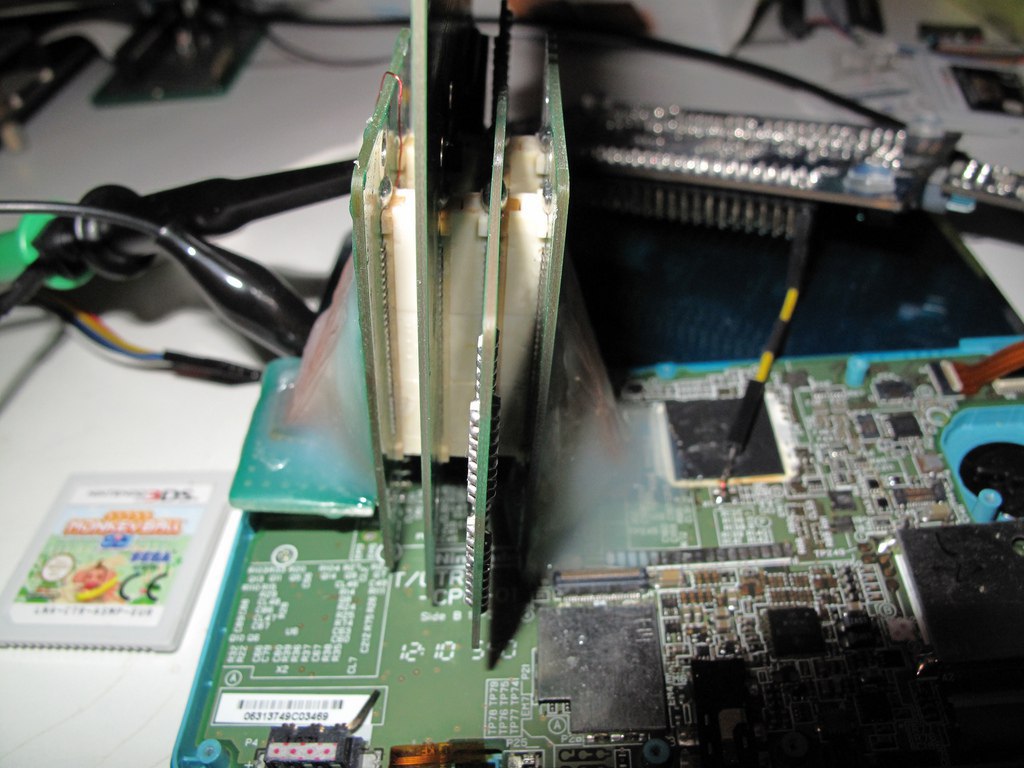
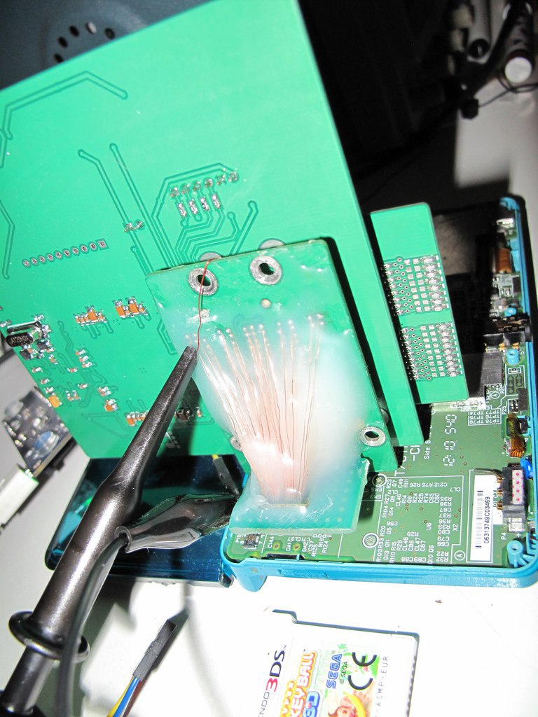
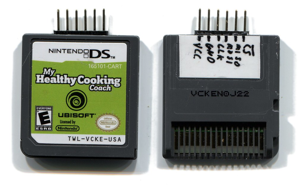
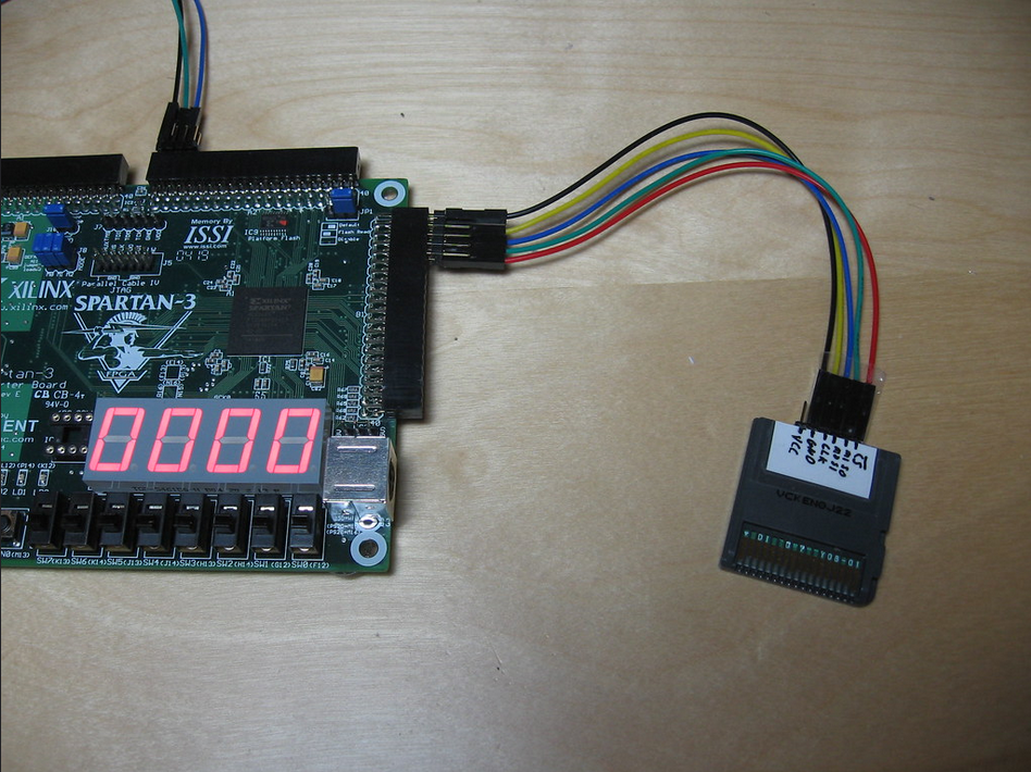
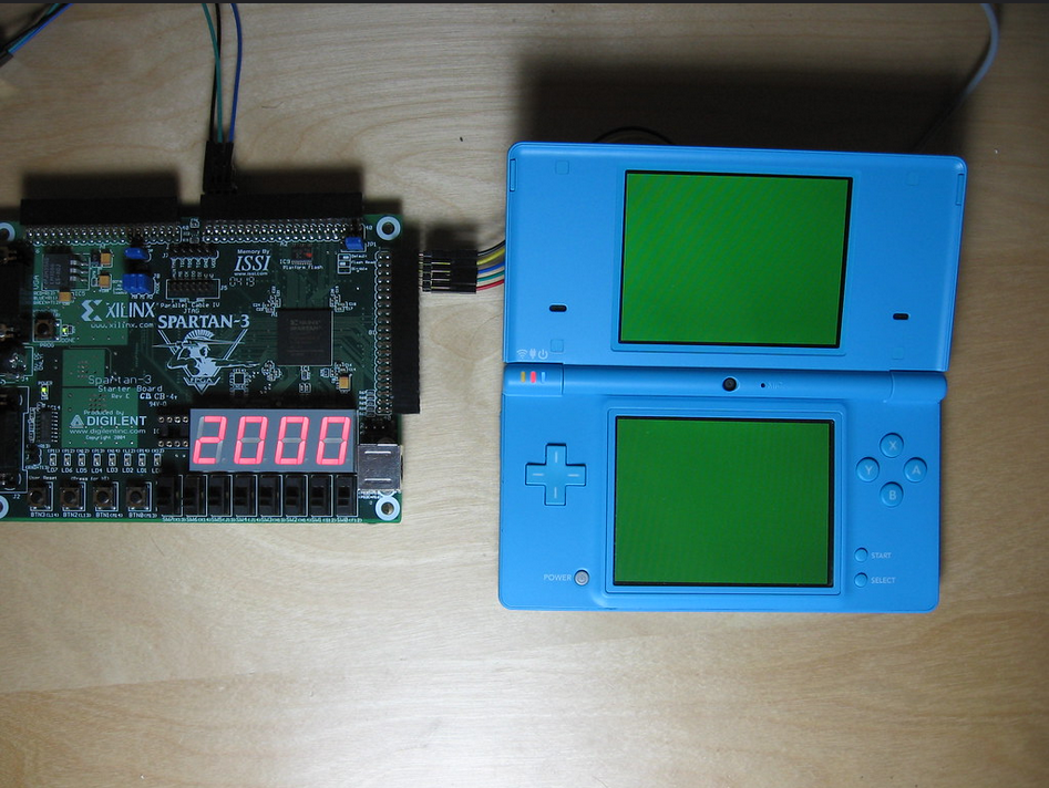
EEPROM Emulation + Savegame Attack
Now this is a quite different attack. It is refreshing because even though it also requires an FPGA, it involves much less soldering, and the work that has to be done is simpler.
17/11/2019 EDIT: Apparently Team Twiizers managed to set up an emulation attack with an Arduino! Check Hacking The 3DS V to see it ;) !
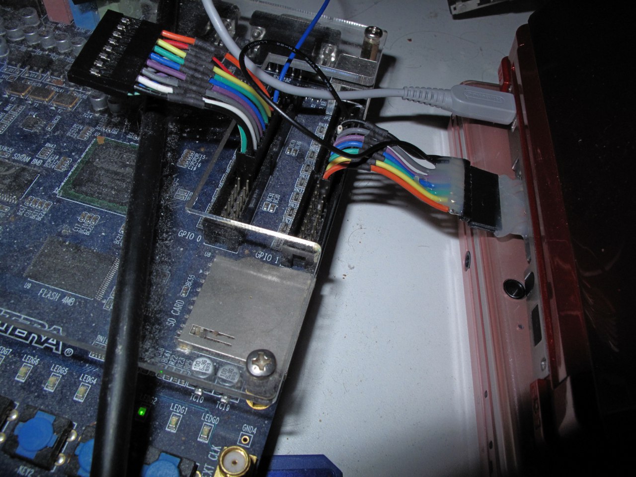
The first implementation I saw of the Emulation Attack was done by Micah Elizabeth Scott (scanlime) and you can see her work here:
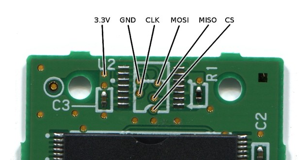
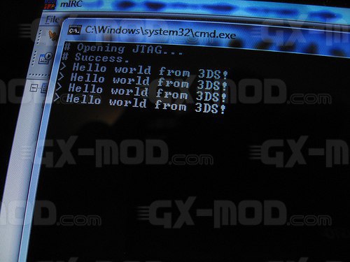
With this setup, it is possible to simulate a cartridge’s savegame EEPROM and “feed” in real time a save to the game. The game’s code uses the savegame as input, so it is a good target for exploits, as we’ll see in later posts.
scanlime’s setup running a DS mode exploit ;)
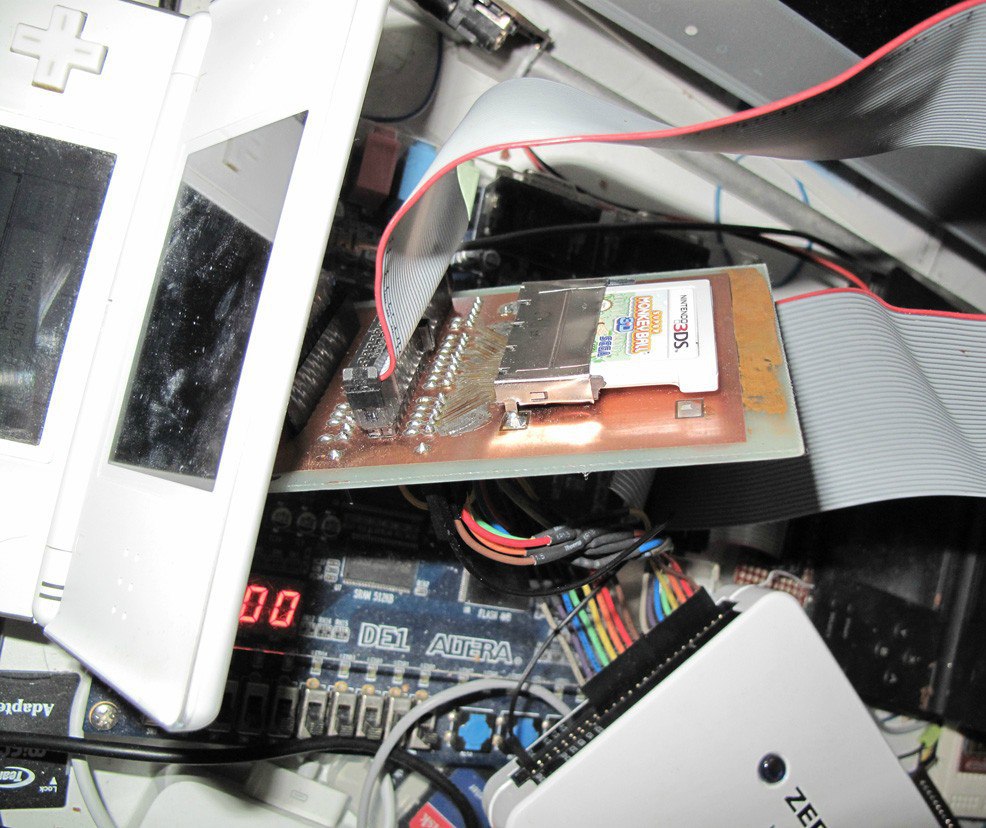
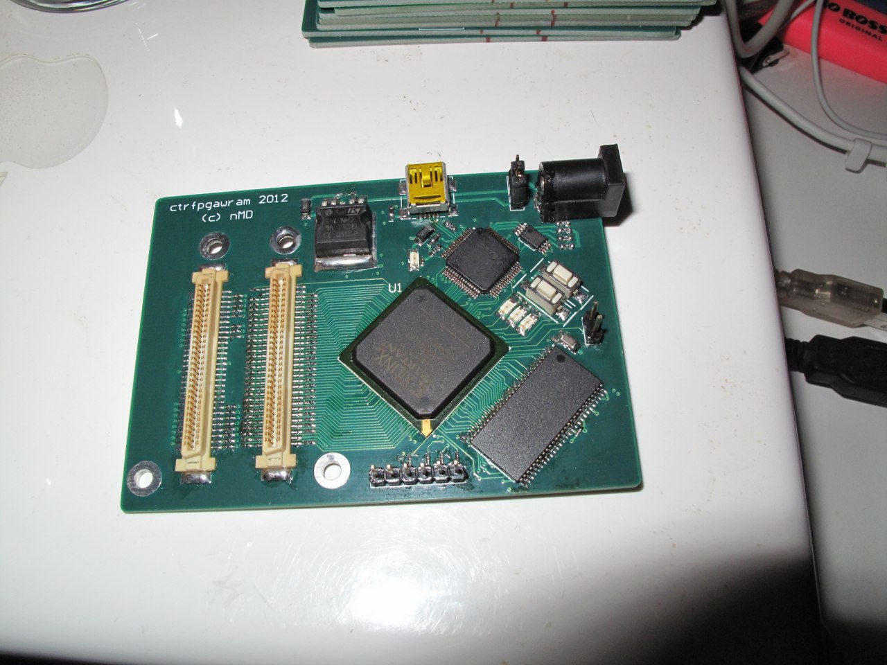
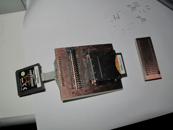
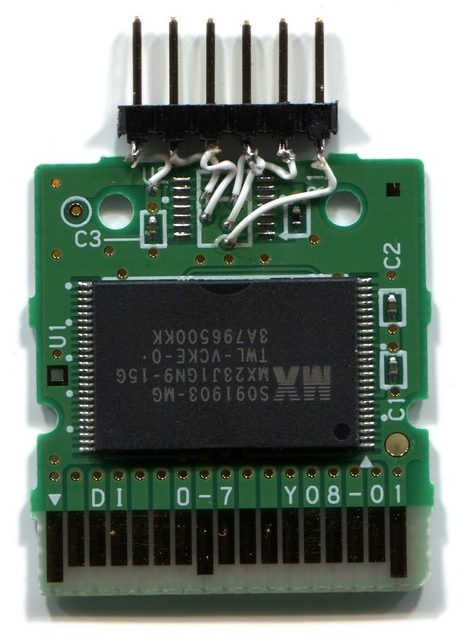
Recently my friend Gericom has been working on a similar interface for NDS, with the subtle difference that his setup emulates the ROM chip as well, thus being able to load NDS and DSi games from his FPGA. He even designed his own PCB instead of refurbishing an actual game cart:
FPGAs are game-changing devices that can interact as virtually any component. The shown interface gives us the power to emulate the EEPROM or ROM chips that interact with the console. Interestingly 3ds cartridges’ internals are 1:1 copies of the NDS ones (with bigger EEPROMs and ROMs, of course), so the attack can be reproduced with 3DS carts. By replacing the content of the EEPROM, which contains the savegame data, we can fuzz data that is inputted into games’ code and find a vulnerability over the savegame.
A FPGA setup build + explanation + code is in progress! As I am building my own interface right now ;)
Glitch attacks / fault injection
This attack vector has, in my humble opinion, the most simple concept yet the most extensive and complex implementations. The idea is to introduce glitches (or faults) into the processor (which is basically a very advanced state machine) so it is possible to skip instructions, change execution flow, dump keys and secrets, etc. There has been successful glitch attacks to the 3DS bootrom in the last years.
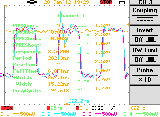
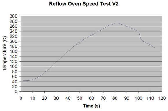
Practical example of a glitch attack.
It is interesting to consider that there exists specific hardware to design and perform glitch attacks, like the Chipwhisperer though it is expensive and usually more extra hardware is needed.
Conclusions
See you soon! Next post I will show how to make a working exploit for backwards compatibility mode, and how to fuzz(attack) native code from there! I am also trying to build a FPGA setup by myself! We are getting close to native 3DS code execution!
Special thanks to @Nitehack (saved all that FPGA RAM content and pics from disappearing!) , @Gericom (invaluable technical help) and @ChampionLeake.